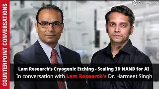
Lam Research’s Cryogenic Etching – Scaling 3D NAND for AI
In the era of on-device AI, the demand for 3D NAND Flash is surging. But as the industry prepares to scale beyond 400 layers, and go to 1,000 layers over the next decade, it introduces a set of challenges for chipmakers. Leading semiconductor equipment maker Lam Research has innovative solutions to help chipmakers with etch and deposition technologies. In the latest Counterpoint Conversations episode, our VP of Research, Neil Shah, had an insightful conversation with Harmeet Singh, Group VP & GM of Etch, Lam Research. Singh shed light on how the industry is pushing the envelope of memory density and performance.
Follow us on social media platforms:
Twitter - / counterpointtr
LinkedIn - / counterpoint-technology-market-research
Instagram - / counterpointresearch
@LamResearchCorp
Смотрите видео Lam Research’s Cryogenic Etching – Scaling 3D NAND for AI онлайн, длительностью часов минут секунд в хорошем качестве, которое загружено на канал Counterpoint Research 28 Август 2024. Делитесь ссылкой на видео в социальных сетях, чтобы ваши подписчики и друзья так же посмотрели это видео. Данный видеоклип посмотрели 23,720 раз и оно понравилось 490 посетителям.