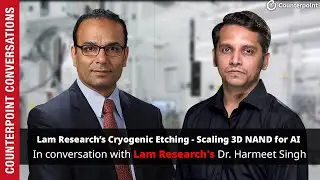
Lam Research’s Cryogenic Etching – Scaling 3D NAND for AI
In the era of on-device AI, the demand for 3D NAND Flash is surging. But as the industry prepares to scale beyond 400 layers, and go to 1,000 layers over the next decade, it introduces a set of challenges for chipmakers. Leading semiconductor equipment maker Lam Research has innovative solutions to help chipmakers with etch and deposition technologies. In the latest Counterpoint Conversations episode, our VP of Research, Neil Shah, had an insightful conversation with Harmeet Singh, Group VP & GM of Etch, Lam Research. Singh shed light on how the industry is pushing the envelope of memory density and performance.
Follow us on social media platforms:
Twitter - / counterpointtr
LinkedIn - / counterpoint-technology-market-research
Instagram - / counterpointresearch
@LamResearchCorp
Watch video Lam Research’s Cryogenic Etching – Scaling 3D NAND for AI online, duration hours minute second in high quality that is uploaded to the channel Counterpoint Research 28 August 2024. Share the link to the video on social media so that your subscribers and friends will also watch this video. This video clip has been viewed 23,720 times and liked it 490 visitors.