How to Clean Polygon Pour between SMD Pads
Tech Consultant Zach Peterson dives into a viewer question relating to making polygon pour between SMD pads appear more professional. Zach details techniques in the PCB footprint and library that reveal how to better control where polygon pour might appear.
0:00 Intro
0:47 The Viewer Question
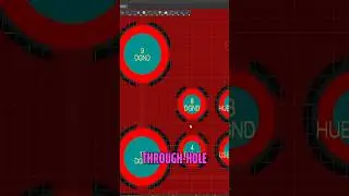
1:54 Cutouts Method
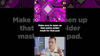
7:40 Design Rules Method
For more PCB Layout videos, click here: • PCB Layout
For more PCB Design for Beginners videos, click here: • PCB Design for Beginners
For more Tech Consultant Zach Peterson videos, click here: • Technical Consultant Zach Peterson
👉 Query Language in Altium Designer: Basic Concepts - Part I: • Query Language in Altium Designer: Ba...
👉 How to Make Polygon Pours and Cutouts More Professional: • How to Make Polygon Pours and Cutouts...
👉 Polygon Pour in Altium Designer: • Polygon Pour in Altium Designer | PCB...
👉 Working with a Polygon Pour Object on a PCB in Altium Designer: https://www.altium.com/documentation/...
👉 15 Days Free Altium Designer Access: http://altium.com/yt/altium-academy
Don't forget to follow us on social to stay up-to-date on the latest Altium Academy content.
👉 Follow Altium on Twitter: / altium
👉 Follow Altium on Linkedin: / altium
👉 Follow Altium on Facebook: / altiumofficial
👉 Ready to try the industry's best-in-class design experience yourself? Download it today and get started! https://www.altium.com/downloads?utm_...
The Altium Academy is an online experience created to bring modern education to PCB Designers and Engineers all across the world. Here you can access a vast library of free training and educational content covering everything from basic design to advanced principles and step-by-step walkthroughs. Join industry legends as they share their career knowledge, review real-life design projects, or learn how to leverage one of Altium's leading design tools. No matter your level of experience, the Altium Academy can help you become a better Designer and Engineer!
About Altium LLC
Altium LLC (ASX:ALU), a global software company based in San Diego, California, is accelerating the pace of innovation through electronics. From individual inventors to multinational corporations, more PCB designers and engineers choose Altium software to design and realize electronics-based products.
#Altium #PCBdesign #ElectronicsDesign
Watch video How to Clean Polygon Pour between SMD Pads online, duration hours minute second in high quality that is uploaded to the channel Altium Academy 01 January 1970. Share the link to the video on social media so that your subscribers and friends will also watch this video. This video clip has been viewed 5,261 times and liked it 135 visitors.